Products
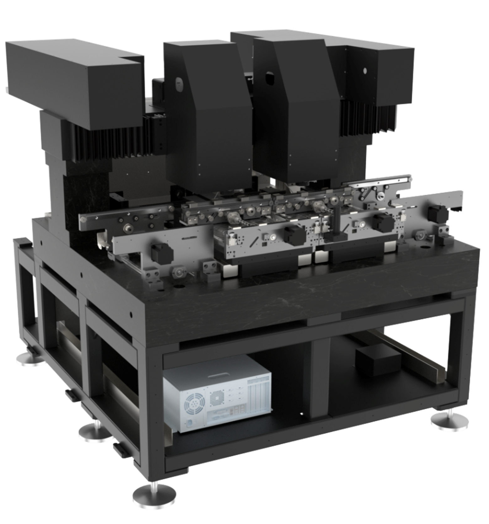
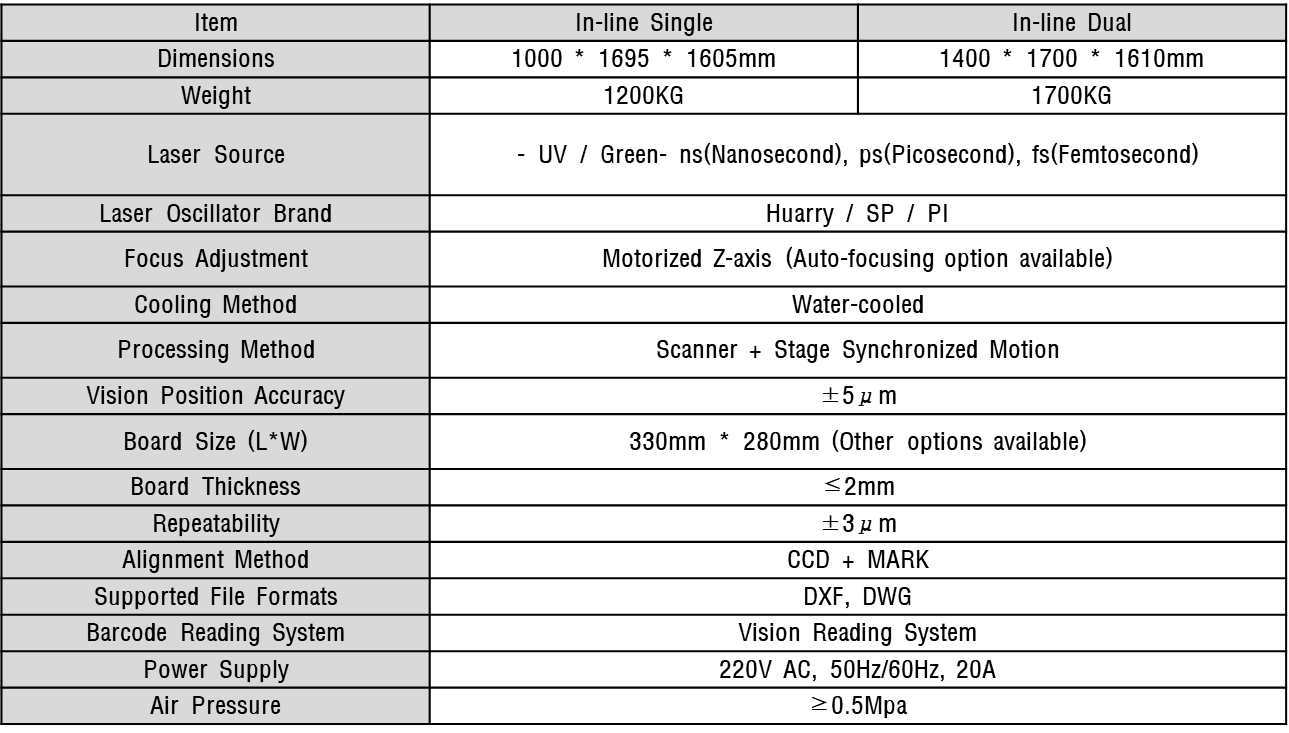
Inline Laser PCB/FPCB Router
- Stress-Free Cutting: Non-contact laser prevents micro-cracks and circuit damage.
- In-line Optimization: Stable interface designed for seamless automated production lines.
- Versatile Laser Sources: Supports various sources including Nano, Pico, and Femto lasers.
- Power Monitoring Option: Real-time laser power measurement for reliable process data.
- Minimal Maintenance: No consumable bits and dust-free operation for cleanroom use.
Product Details
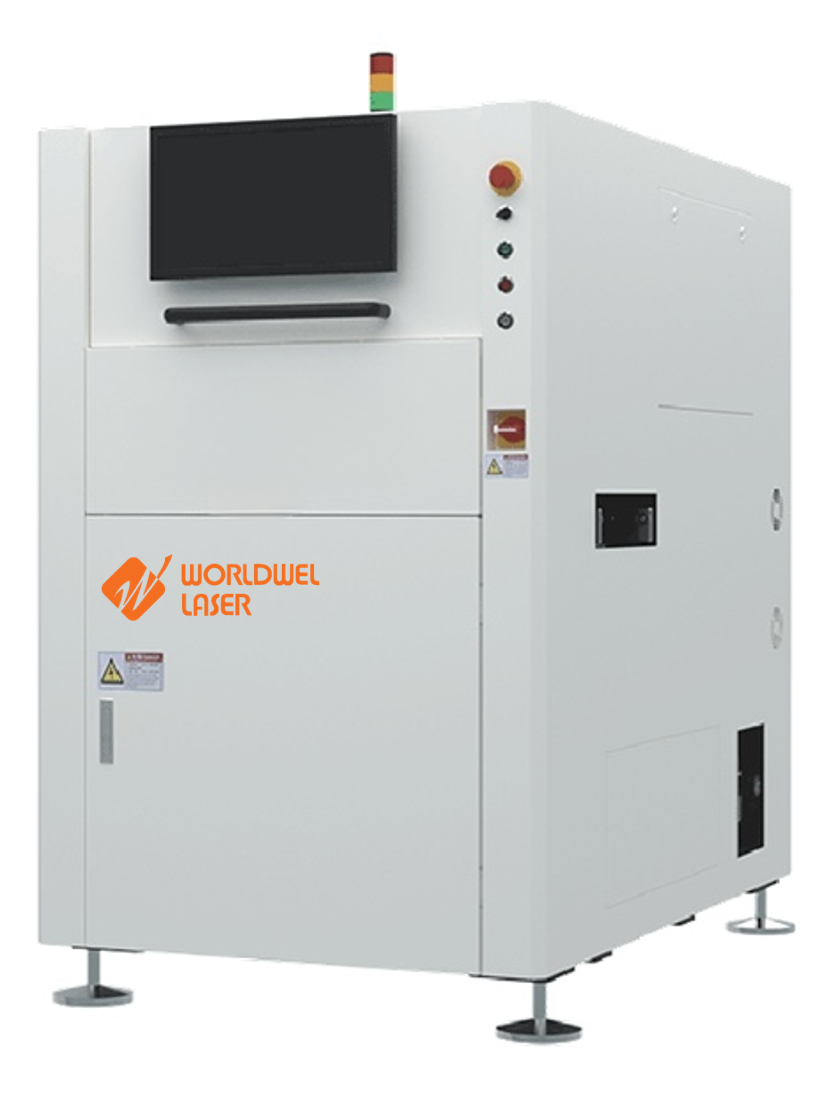
1. Superior Precision & Repeatability
Exceptional Process Capability (Cp/Cpk): Achieves a Cp of 2.00, significantly outperforming traditional routers (Cp 0.59) for near-zero defect production.
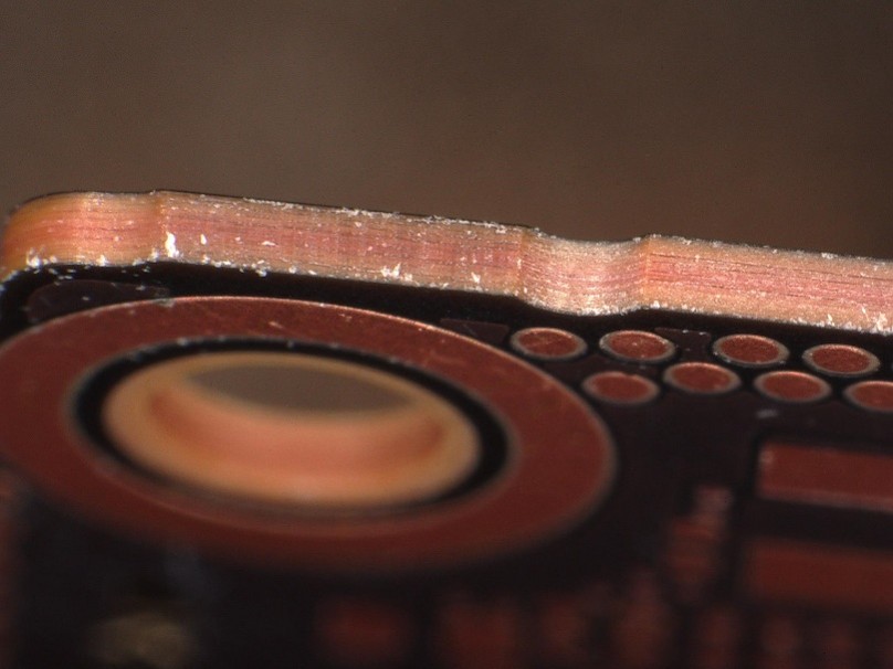
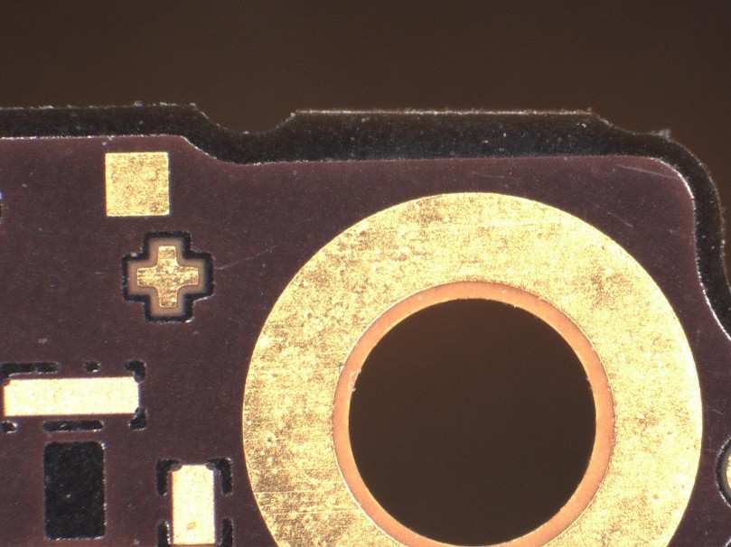
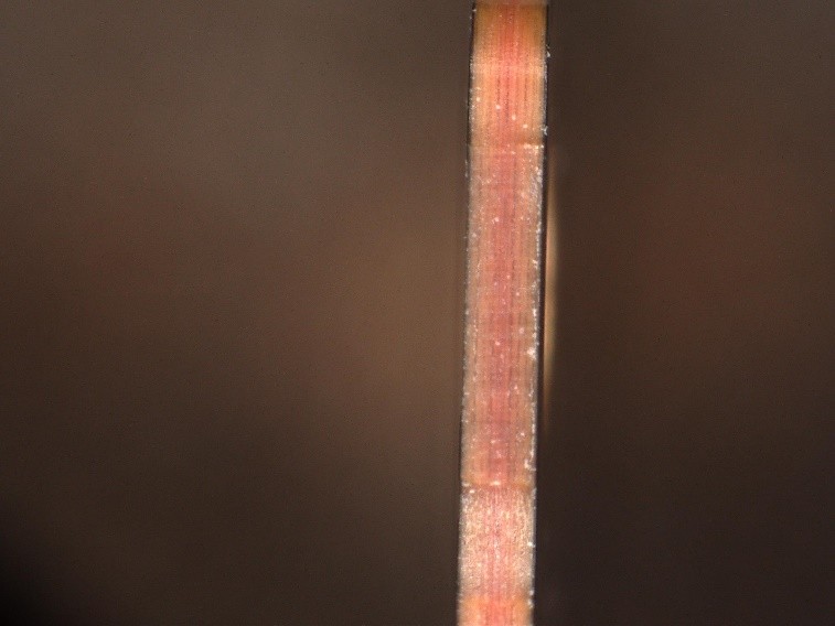
Ultra-Narrow Gap Cutting: Supports cutting distances as small as 0.08mm , allowing for 20-40% more space in high-density PCB designs compared to mechanical bits.
2. Advanced Thermal Management
Low-Temperature Processing: Maintains surface temperatures below 64°C (vs. 150°C in routers), ensuring zero thermal damage to sensitive SMT components and micro-circuits.
Minimized HAZ (Heat-Affected Zone): Prevents discoloration and warping, making it ideal for multi-layer and Flex-Rigid PCB applications.
3. Enhanced Signal Integrity & Design Freedom
Noise & Vibration Control: Non-contact processing eliminates mechanical stress, maintaining signal integrity and reducing crosstalk for high-speed data transmission.
Complex Geometry Support: No constraints on bit diameter; easily processes curves, sharp angles, and custom shapes without molds, shortening the R&D cycle by up to 70%.
4. Maximum Efficiency & Cost Reduction
95% Material Utilization: The ultra-fine laser beam (0.02-0.1mm) minimizes waste, maximizing board usage and reducing production costs.
Maintenance-Free Operation: Eliminates the need for tool changes and manual recalibration. Fully smart factory-ready with MES integration and automated vision compensation.
Spec.